- 您现在的位置:买卖IC网 > Sheet目录1193 > AD8348-EVALZ (Analog Devices Inc)BOARD EVAL FOR AD8348
�� �
�
�AD8348�
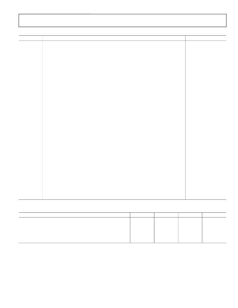
�Table� 6.� Evaluation� Board� Configuration� Options�
�Component�
�V� S� ,� GND�
�SW11,� ENBL�
�SW13,� R15,�
�VGIN�
�SW12�
�IFIP,� R31,� R32�
�MXIP,� MXIN,�
�T41,�
�R41,� R42,�
�C42,� C43�
�LK11,� VCMO�
�C8,� C9,� R4,� R5�
�(I� and� Q)�
�C10� (I� and� Q)�
�C1� to� C7,�
�R1,� R2,�
�L1� to� L3�
�(I� and� Q)�
�LK5� (I� and� Q)�
�Function�
�Power� supply� and� ground� vector� pins.�
�Device� enable:� Place� SW11� in� the� ENBL� position� to� connect� the� ENBL� pin� to� V� S� .� Place� SW11� in�
�the� DENBL� position� to� disable� the� device� by� grounding� the� Pin� ENBL� through� a� 50� Ω� pull-down�
�resistor.� The� device� can� also� be� enabled� via� an� external� voltage� applied� to� ENBL� or� VENB.�
�Gain� control� selection:� With� SW13� in� the� POT� position,� the� gain� of� the� VGA� can� be� set� using� the�
�R15� potentiometer.� With� SW13� in� the� EXT� position,� the� VGA� gain� can� be� set� by� an� external�
�voltage� to� the� SMA� connector� VGIN.� For� VGA� operation,� the� VGA� must� first� be� enabled� by�
�setting� SW12� to� the� IF� position.�
�VGA� enable� selection:� With� SW12� in� the� IF� position,� the� ENVG� pin� is� connected� to� V� S� and� the�
�VGA� is� enabled.� The� IF� input� should� be� used� when� SW12� is� in� the� IF� position.� With� SW12� in� the�
�MX� position,� the� ENVG� pin� is� grounded� and� the� VGA� is� disabled.� The� MX� inputs� should� be� used�
�when� SW12� is� in� the� MX� position.�
�IF� inputs:� The� single-ended� IF� signal� should� be� connected� to� this� SMA� connector.� R31� and� R32�
�form� an� L� pad� that� presents� a� 50� Ω� termination� to� the� driving� source.� This� L� pad� introduces� an�
�11.46� dB� loss� in� the� input� signal� path� and� should� be� taken� into� consideration� when� calculating�
�the� gain� of� the� AD8348.�
�Mixer� inputs:� These� inputs� can� be� configured� for� either� differential� or� single-ended� operation.�
�The� evaluation� board� is� by� default� set� for� differential� MX� drive� through� a� balun� (T41)� from� a�
�single-ended� source� fed� into� the� MXIP� SMA� connector.� To� change� to� a� differential� driving� source,�
�T41� should� be� removed� along� with� Resistor� R42.� The� 0� Ω� Resistors� R43� and� R44� should� be� installed� in�
�place� of� T41� to� bridge� the� gap� between� the� input� traces.� This� will� present� a� nominal� differential�
�impedance� of� 200� Ω� (100� Ω� per� side).� The� differential� inputs� should� then� be� fed� into� SMA�
�connectors� MXIP� and� MXIN.�
�Baseband� amplifier� output� bias:� Installing� LK11� connects� VREF� to� VCMO.� This� sets� the� bias� level�
�on� the� baseband� amplifiers� to� VREF,� which� is� equal� to� approximately� 1� V.� Alternatively,� with�
�LK11� removed,� the� bias� level� of� the� baseband� amplifiers� can� be� set� by� applying� an� external�
�voltage� to� the� VCMO� test� point.�
�Baseband� amplifier� outputs� and� output� filter:� Additional� low-pass� filtering� can� be� provided� at�
�the� baseband� output� with� these� filters.�
�Mixer� output� dc-blocking� capacitors:� The� mixer� outputs� are� biased� to� VCMO.� To� prevent�
�damage� to� test� equipment� that� cannot� tolerate� dc� biases,� C10� is� provided� to� block� the� dc�
�component,� thus� protecting� the� test� equipment.�
�Baseband� filter:� These� components� are� provided� for� baseband� filtering� between� the� mixer�
�outputs� and� the� baseband� amplifier� inputs.� The� baseband� amplifier� input� impedance� is� high�
�and� the� filter� termination� impedance� is� set� by� R2.� See� Table� 7� for� the� jumper� settings.�
�Offset� compensation� loop� disable:� Installing� these� jumpers� will� disable� the� offset� compensation�
�Default� Condition�
�Not� applicable�
�SW11� =� ENBL�
�SW13� =� POT�
�SW12� =� IF�
�R31� =� 57.6� Ω�
�R32� =� 174� Ω�
�T41� =� M/A-COM� ETK4-2T;�
�R41=� OPEN;� C42,� C43� =�
�1000� pF;� R42� =� 0� Ω�
�LK11� installed�
�R4,� R5� =� 0� Ω�
�C10� =� 0� Ω�
�All� =� OPEN�
�LK5x� =� OPEN�
�loop� for� the� corresponding� channel.�
�Table� 7.� Filter-Jumper� Configuration� Options�
�Condition�
�LK1x�
�LK2x�
�LK3x�
�LK4x�
�xMXO� to� xAIN� Directly�
�xMXO� to� xAIN� via� Filter�
�xMXO� to� J1x� Directly,� xAIN� Unused�
�xMXO� to� J1x� via� Filter,� xAIN� Unused�
�Drive� xAIN� from� J1x�
�?�
�?�
�Rev.� A� |� Page� 27� of� 28�
�?�
�?�
�?�
�?�
�?�
�?�
�?�
�发布紧急采购,3分钟左右您将得到回复。
相关PDF资料
AD8436-EVALZ
BOARD EVAL FOR AD8436
AD9352-5/PCBZ
EVALUATION BOARD
AD9550/PCBZ
BOARD EVALUATION FOR AD9550
AD9985A/PCBZ
KIT EVALUATION FOR AD9985A
ADA4850-2YCP-EBZ
BOARD EVAL FOR ADA4850-2YCP
ADA4899-1YCP-EBZ
BOARD EVAL FOR ADA4899-1YCP
ADA4937-1YCP-EBZ
BOARD EVAL FOR ADA4937-1YCP
ADA4938-2YCP-EBZ
BOARD EVAL FOR ADA4938-2YCP
相关代理商/技术参数
AD8348XRU
制造商:Analog Devices 功能描述:QUADRATURE MODULATOR X-GRADE - Rail/Tube
AD8348XXX
制造商:AD 制造商全称:Analog Devices 功能描述:50-1000 MHz Quadrature Demodulator
AD8349
制造商:AD 制造商全称:Analog Devices 功能描述:400 MHz to 6 GHz Broadband Quadrature Modulator
AD8349ARE
制造商:Analog Devices 功能描述:Quadrature Mod 160MHz 16-Pin TSSOP EP Tube 制造商:Rochester Electronics LLC 功能描述:DIRECT QUADRATURE MODULATOR - Bulk 制造商:Analog Devices 功能描述:IC MODULATOR QUADRATURE
AD8349ARE-REEL7
功能描述:IC QUADRATURE MOD 700MHZ 16TSSOP RoHS:否 类别:RF/IF 和 RFID >> RF 调制器 系列:- 产品培训模块:Lead (SnPb) Finish for COTS
Obsolescence Mitigation Program 标准包装:2,500 系列:- 功能:调制器 LO 频率:700MHz ~ 2.3GHz RF 频率:700MHz ~ 2.3GHz P1dB:1dBm 底噪:-148dBm/Hz 输出功率:-1dBm 电流 - 电源:46mA 电源电压:2.7 V ~ 3.6 V 测试频率:1.75GHz 封装/外壳:28-WFQFN 裸露焊盘 包装:带卷 (TR)
AD8349AREZ
功能描述:IC QUADRATURE MOD 700MHZ 16TSSOP RoHS:是 类别:RF/IF 和 RFID >> RF 调制器 系列:- 产品培训模块:Lead (SnPb) Finish for COTS
Obsolescence Mitigation Program 标准包装:2,500 系列:- 功能:调制器 LO 频率:700MHz ~ 2.3GHz RF 频率:700MHz ~ 2.3GHz P1dB:1dBm 底噪:-148dBm/Hz 输出功率:-1dBm 电流 - 电源:46mA 电源电压:2.7 V ~ 3.6 V 测试频率:1.75GHz 封装/外壳:28-WFQFN 裸露焊盘 包装:带卷 (TR)
AD8349AREZ-RL7
功能描述:IC MOD QUAD 2.7GHZ 16TSSOP RoHS:是 类别:RF/IF 和 RFID >> RF 调制器 系列:- 产品培训模块:Lead (SnPb) Finish for COTS
Obsolescence Mitigation Program 标准包装:2,500 系列:- 功能:调制器 LO 频率:700MHz ~ 2.3GHz RF 频率:700MHz ~ 2.3GHz P1dB:1dBm 底噪:-148dBm/Hz 输出功率:-1dBm 电流 - 电源:46mA 电源电压:2.7 V ~ 3.6 V 测试频率:1.75GHz 封装/外壳:28-WFQFN 裸露焊盘 包装:带卷 (TR)
AD8349EVAL
制造商:Analog Devices 功能描述:IC ((NS))